
Introduction
While design and fabrication receive much of the spotlight in the semiconductor industry, manufacturing and packaging are the final yet vital steps that bring a chip to life. Without these processes, even the most advanced chip designs would remain unusable. From wafer dicing to 3D packaging, this domain is full of technical depth and career opportunities.
Let me walk you through the importance of manufacturing and packaging, the career landscape, and how you can prepare to enter this exciting segment.
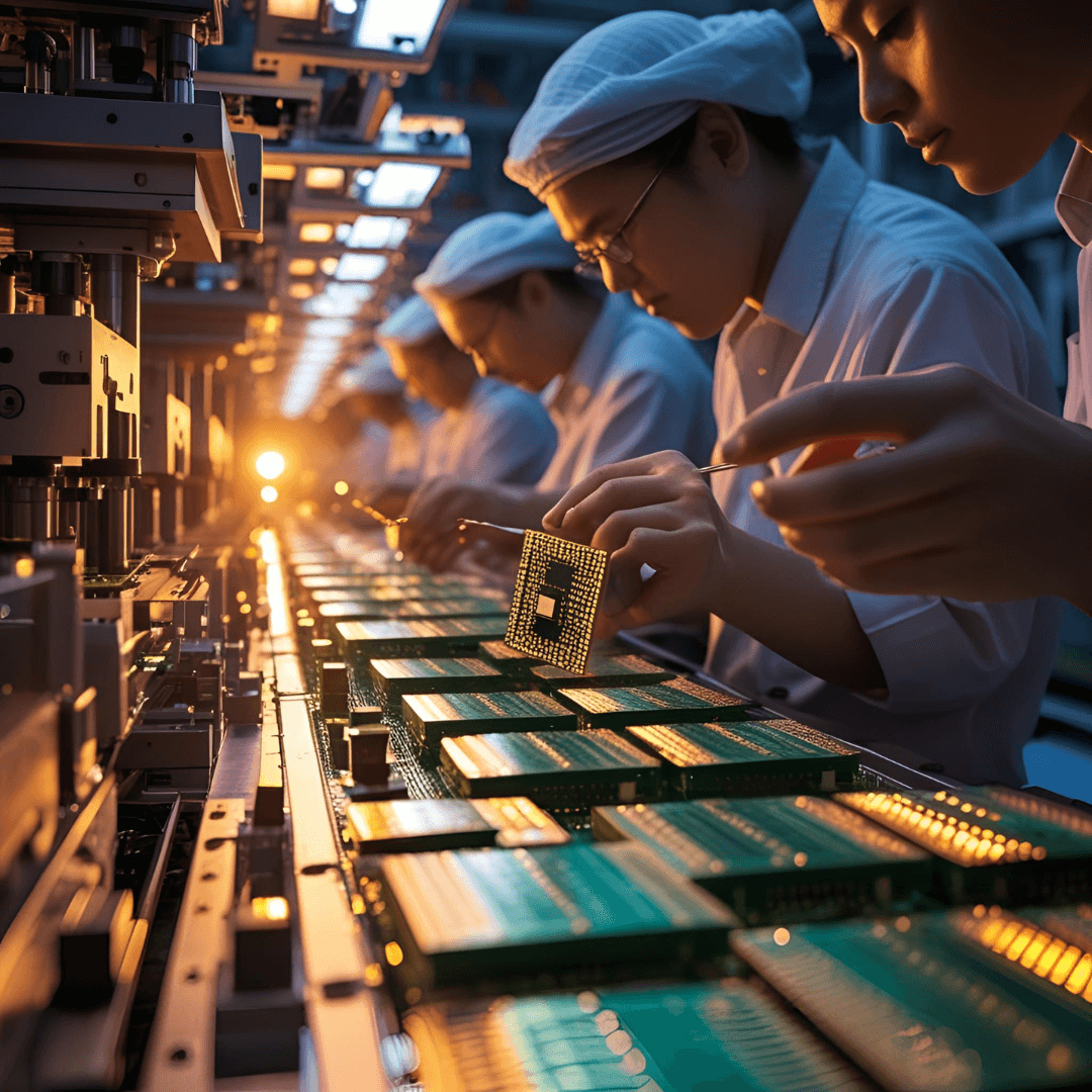
Manufacturing in semiconductors refers to the back-end processes following wafer fabrication, including wafer thinning, testing, dicing, and assembly. Packaging involves enclosing the chip in a protective casing while ensuring connectivity with the external world via pins, balls, or pads.
Some of the leading players in this domain include:
These companies serve fabless design firms and IDMs alike.
Manufacturing and packaging companies serve as the final step in the semiconductor value chain. Their core functions include:
They also ensure quality testing, yield enhancement, and reliability for real-world operation.
Here’s a breakdown of what companies typically look for:
Skills in process optimization and statistical process control (SPC) are a big plus.
Preparation for a career in packaging and manufacturing involves a mix of theory and hands-on exposure:
A proactive approach makes a big difference in this competitive domain.
The job ecosystem in this space is wide-ranging and impactful:
These roles support high reliability, cost-effective delivery of every IC.
A Layout Engineer plays a crucial preparatory role before the chip enters the manufacturing stage:
In short, layout quality directly affects packaging efficiency and yield.
The Semionics IC Layout Design course offers more than just layout training. Here’s why it’s valuable for packaging aspirants too:
It’s the perfect stepping stone into a career that connects both design and physical realization.
Use any of the following channels to begin your journey with us:
Manufacturing and packaging may be the last steps in the IC journey, but they determine product quality, performance, and life span. With advanced packaging gaining momentum — from chiplets to 3D integration — the future is full of innovation.
Be a part of it with the right skills. Let Semionics help you take the first step toward a career that shapes the future of electronics.
Semionics – Your global partner for VLSI upskilling and ASIC signoff expertise.

Semionics, Your Partner in semiconductor space , connecting industry needs with skilled professionals in Analog & Mixed-Signal IC Layout Design and Physical Verification ."from Basics to Brilliance .. A path to Semiconductor Industry!!"