
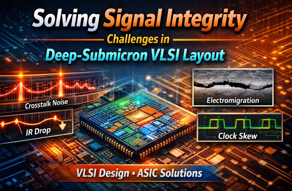
As we moved from micron technologies to deep-submicron layout nodes like 28nm, 14nm, and below, something fundamental changed. Transistors became faster. Supply voltages dropped. However, interconnects began to dominate delay.
In modern VLSI physical design, wires are no longer passive metal connections. Instead, they behave like distributed RC networks. In fact, parasitic resistance and capacitance now significantly impact signal integrity, timing closure, and overall chip reliability.
So what is signal integrity?
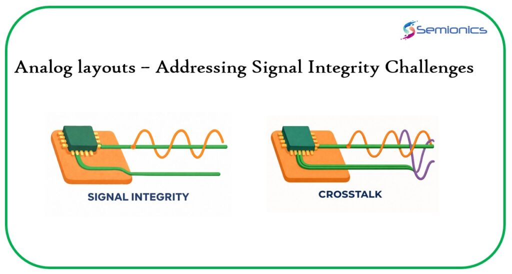
Simply put, signal integrity (SI) refers to the quality of an electrical signal as it travels from source to destination without distortion, excessive delay, or noise corruption.
However, in deep-submicron nodes:
Therefore, SI is no longer optional. It is central to successful ASIC design, SoC layout, and high-speed chip implementation.
Let us simplify this.
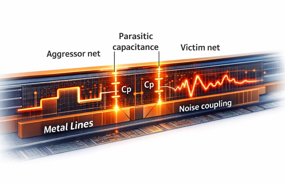
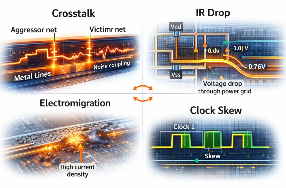
When metal lines are placed very close to each other, capacitive coupling increases. As a result, switching on one net injects noise into a neighboring quiet net. This is known as crosstalk noise.
Now imagine a critical clock net running adjacent to a high-activity data bus. The induced noise can cause:
Similarly, IR drop occurs when the power grid cannot sustain required current. Consequently, transistors do not receive full supply voltage. This leads to performance degradation.
Furthermore, electromigration (EM) becomes critical in advanced nodes. High current density gradually displaces metal atoms. Eventually, open circuits may occur.
Clock networks also suffer. In high-performance designs, even a few picoseconds of skew can break timing closure.
Thus, signal integrity challenges are interconnected. They affect power integrity, timing analysis, and reliability engineering.
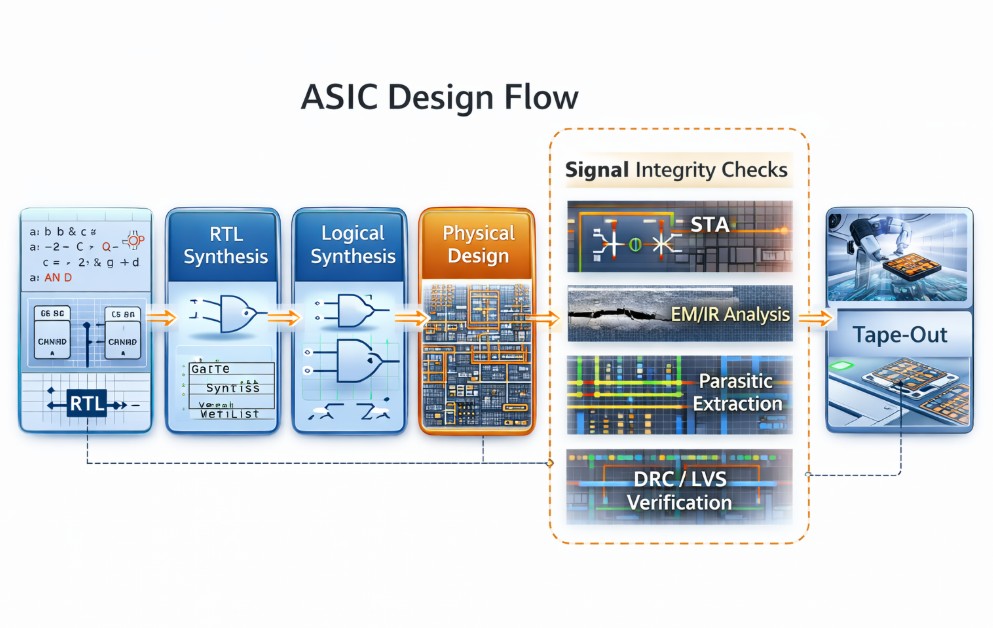
Now comes the most important part. How do we solve these problems in real chip design projects?
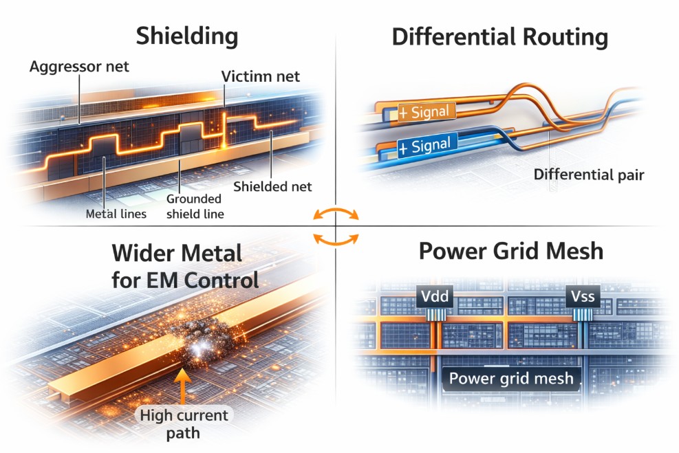
Adding grounded shield lines between aggressor and victim nets significantly reduces coupling noise.
Increasing spacing between critical nets minimizes parasitic capacitance.
In high-speed blocks, differential pairs improve noise immunity and reduce common-mode interference.
A well-designed mesh reduces IR drop and improves power integrity.
Using wider metals for high-current paths prevents electromigration failures.
Modern EDA tools integrate SI analysis during static timing analysis (STA). Therefore, timing signoff must include noise-aware simulations.
In real industry projects, solving SI is not about theory alone. It requires collaboration between circuit designers, layout engineers, and verification teams.
This is where industry exposure becomes invaluable.
During chip tape-out, every parasitic matters.
At this stage:
However, many young engineers learn theory without seeing how these checks interact in real silicon.
That gap between classroom knowledge and silicon reality is where most failures occur.
Deep-submicron signal integrity is not just a layout topic. It is a system-level challenge that blends:
Therefore, mastering SI means understanding the full ASIC design flow.
In deep-submicron technologies, scaling brings performance. However, it also brings vulnerability.
A single overlooked coupling path can break functionality. A poorly designed power grid can reduce yield. A minor clock skew can cost millions in re-spins.
As semiconductor professionals and aspiring VLSI engineers, we must ask ourselves:
Are we designing for functionality alone, or are we designing for robustness, reliability, and manufacturability?
Signal integrity is no longer a back-end correction step. It is a design philosophy.
If you truly want to understand advanced signal integrity analysis, real-world ASIC physical design challenges, and industry-grade layout methodologies, I strongly encourage you to explore structured, application-oriented learning resources at:
Click the Link to access the Full course on 👉 academy.semionics.com
https://academy.semionics.com/courses/Analog-Layouts—Addressing-Signal-Integrity-Challenges-6989d4cd2d75492c078acc59
Additionally, visit www.semionics.com to explore more knowledge-driven semiconductor content designed specifically for industry professionals and ambitious engineering talent.
The images and content used in this blog are generated, created, or referenced from Google Images and other educational sources. They are intended purely for educational and guidance purposes, with no intention of monetization. All credits belong to the respective owners. Semionics holds no responsibility for third-party content and encourages readers to verify before use.

Semionics, Your Partner in semiconductor space , connecting industry needs with skilled professionals in Analog & Mixed-Signal IC Layout Design and Physical Verification ."from Basics to Brilliance .. A path to Semiconductor Industry!!"