

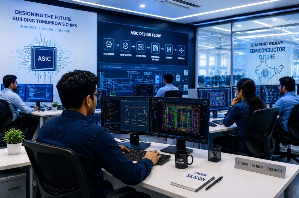
India is no longer just a software powerhouse. It is rapidly becoming a global hub for semiconductor design and VLSI innovation. With increasing investments, government initiatives, and global companies expanding design centers, the demand for skilled VLSI engineers in India (2026) is at an all-time high.
However, there is a gap. While thousands graduate every year, only a small percentage are industry-ready. This is not due to lack of intelligence. Rather, it is due to lack of practical exposure in ASIC design, physical design, and verification flows. Therefore, choosing the best VLSI course in India is not just about learning tools. It is about learning how real chips are designed, verified, and taped out.
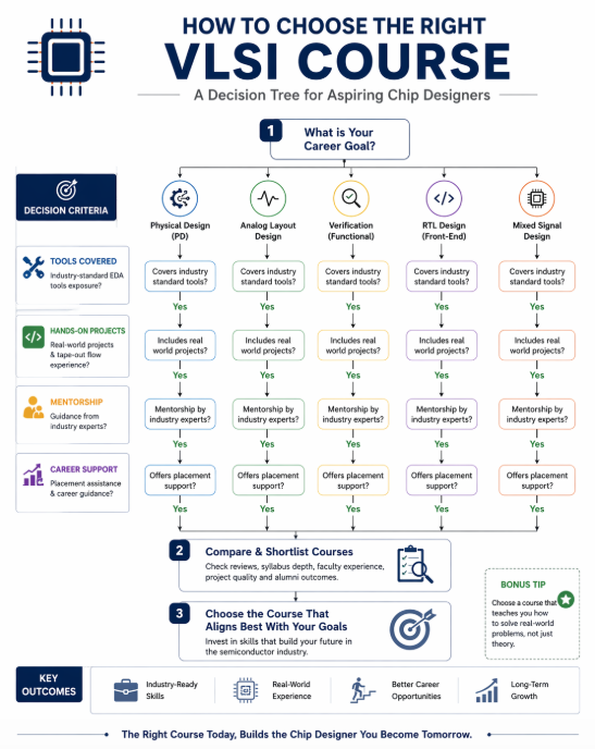
Let’s break a myth. A “good course” is not defined by duration or marketing claims. Instead, it is defined by how closely it aligns with real semiconductor industry workflows.
The best VLSI training institutes in India must offer:
Moreover, strong mentorship plays a key role. Learning from engineers who have worked on real silicon significantly accelerates understanding.
“Create an educational infographic showing ASIC design flow from RTL to GDSII, including synthesis, placement, routing, STA, DRC, LVS. Clean white background, labeled steps.”
Depending on your interest and career goals, VLSI courses can be broadly categorized:
Focuses on placement, routing, clock tree synthesis, and timing closure. Highly in demand in ASIC companies.
Covers transistor-level design, matching techniques, and layout-dependent effects. Critical for AMS (Analog Mixed Signal) roles.
Involves functional validation using methodologies like UVM. Essential for ensuring design correctness.
Covers Verilog/SystemVerilog coding and synthesis.
Combines analog and digital design concepts. Requires deeper understanding but offers niche opportunities.
Choosing the right specialization depends on your background. However, industry trends clearly show increasing demand in physical design and analog layout
Now let’s talk about what truly makes a difference.
Among the growing number of training providers, Semionics has positioned itself as a highly practical, industry-focused learning platform.
Here’s why:
Courses are designed based on real ASIC project flows, not academic theory.
Students work on real design examples such as OPAMP layout, routing strategies, and verification flows.
Unlike generic courses, Semionics emphasizes analog layout, physical verification, and backend design, which are highly demanded.
Through academy.semionics.com, learners across India and globally can access structured content.
A growing ecosystem of learners, professionals, and mentors enables continuous growth.
In an industry where practical exposure defines employability, platforms like Semionics bridge the gap effectively.

Before enrolling, ask yourself:
Additionally, always verify course content depth. Avoid programs that focus only on slides or theory. The semiconductor industry values problem-solving ability, not just certifications.
The best VLSI course is not the one with the biggest advertisement. It is the one that changes how you think about circuits, layouts, and real chip challenges.
As we move toward advanced nodes and AI-driven hardware, engineers must evolve beyond basics.
The question is no longer:
“Which course should I take?”
Instead, ask:
👉 “Will this course prepare me to design real silicon?”
If you are serious about building a strong foundation in VLSI design, physical design, and analog layout, explore structured, industry-aligned learning at:
👉 academy.semionics.com
Also, visit www.semionics.com to explore in-depth semiconductor learning resources and career-focused programs.
The images and content used in this blog are generated, created, or referenced from Google Images and other educational sources. They are intended purely for educational and guidance purposes, with no intention of monetization. All credits belong to the respective owners. Semionics holds no responsibility for third-party content and encourages readers to verify before use.

Semionics, Your Partner in semiconductor space , connecting industry needs with skilled professionals in Analog & Mixed-Signal IC Layout Design and Physical Verification ."from Basics to Brilliance .. A path to Semiconductor Industry!!"