

Every layout engineer has faced this paradox — your design passes Design Rule Check (DRC) flawlessly, yet fails timing, leakage, or drive strength tests on silicon.
One of the often-overlooked culprits behind such anomalies is the Poly Cut Effect (PCE).
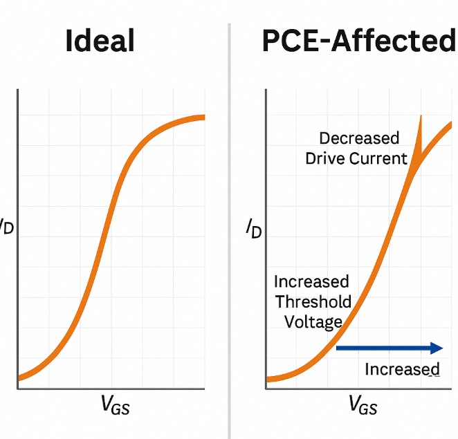
While the term may sound benign, the Poly Cut layer can silently alter transistor performance by modifying gate dimensions, effective channel width, and even threshold voltage (Vth).
As technology nodes shrink below 45nm, even a few nanometers of misalignment or variation in poly cut geometry can cause significant electrical impact.
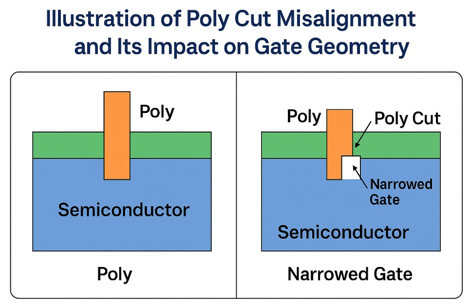
The Poly Cut Effect (PCE) arises due to partial or asymmetric trimming of polysilicon gates during fabrication.
This layer, meant to define gate length and isolate adjacent transistors, can inadvertently shift the effective channel boundary, leading to mismatch between simulated and actual device behavior.
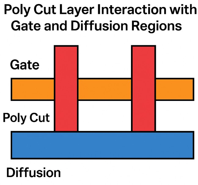
In advanced CMOS technologies, the poly cut (PCUT) defines where the polysilicon gate ends and where the contact and diffusion regions begin.
Even slight deviations in etch bias or alignment can result in:
“The Poly Cut layer may be invisible in your LVS reports, but its effects echo through your timing paths.”
Foundries often issue warnings or Design for Manufacturability (DFM) guidelines around PCE — not because the layout violates rules, but because it violates symmetry.
In analog and mixed-signal blocks, uneven poly cuts near matched transistors cause systematic mismatches.
In digital designs, marginal timing violations and drive strength degradation can appear even when all checks are “green.”
Key foundry alerts include:
These conditions increase the susceptibility of circuits to lithography distortions, making DRC-clean designs functionally unpredictable on silicon.

The Poly Cut Effect doesn’t appear in the schematic — it manifests only after layout.
Its electrical implications ripple across multiple design domains:
“PCE is not a violation — it’s an unmodeled imperfection.”
Mitigating PCE starts with layout awareness and geometry uniformity.
While no single fix exists, the following practices are industry-proven:
At Semionics Academy, PCE isn’t just a textbook term — it’s a real-world design case study.
The Academy’s Layout Nuggets series and interactive learning modules dive into why poly cut effects occur, how they alter device physics, and how to mitigate them in actual designs.
“At Semionics, you don’t just learn layout — you learn what makes or breaks it in silicon.”
As semiconductor nodes continue to scale below 5nm, non-ideal effects like PCE become central to performance, not peripheral.
Designers who understand these nuances create layouts that are manufacturable, reliable, and predictable — the true hallmarks of professional IC design.
Semionics continues to pioneer accessible, industry-ready education that helps engineers move beyond “tool usage” into real layout insight. By merging EDA expertise and hands-on learning, Semionics prepares designers who don’t just follow rules — they understand them.
“A layout that respects physics will always outperform one that just passes DRC.”
📞 Connect with Semionics
The images and content used in this blog are generated, created, or referenced from Google Images and other educational sources. They are intended purely for educational and guidance purposes, with no intention of monetization. All credits belong to the respective owners. Semionics holds no responsibility for third-party content and encourages readers to verify before use.

Semionics, Your Partner in semiconductor space , connecting industry needs with skilled professionals in Analog & Mixed-Signal IC Layout Design and Physical Verification ."from Basics to Brilliance .. A path to Semiconductor Industry!!"