
Every experienced layout engineer knows that design rule clean doesn’t always mean silicon-perfect.
You may have executed a flawless analog layout, verified the LVS, and even passed DFM checks — yet your measured performance drifts beyond expectations. One subtle but critical reason behind such layout-induced variations is the Active Area Space Effect (AAS). Often ignored in early design reviews, AAS quietly alters device behavior by influencing stress distribution, oxide thickness, and doping uniformity across diffusion regions.
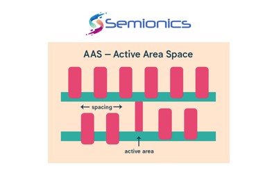
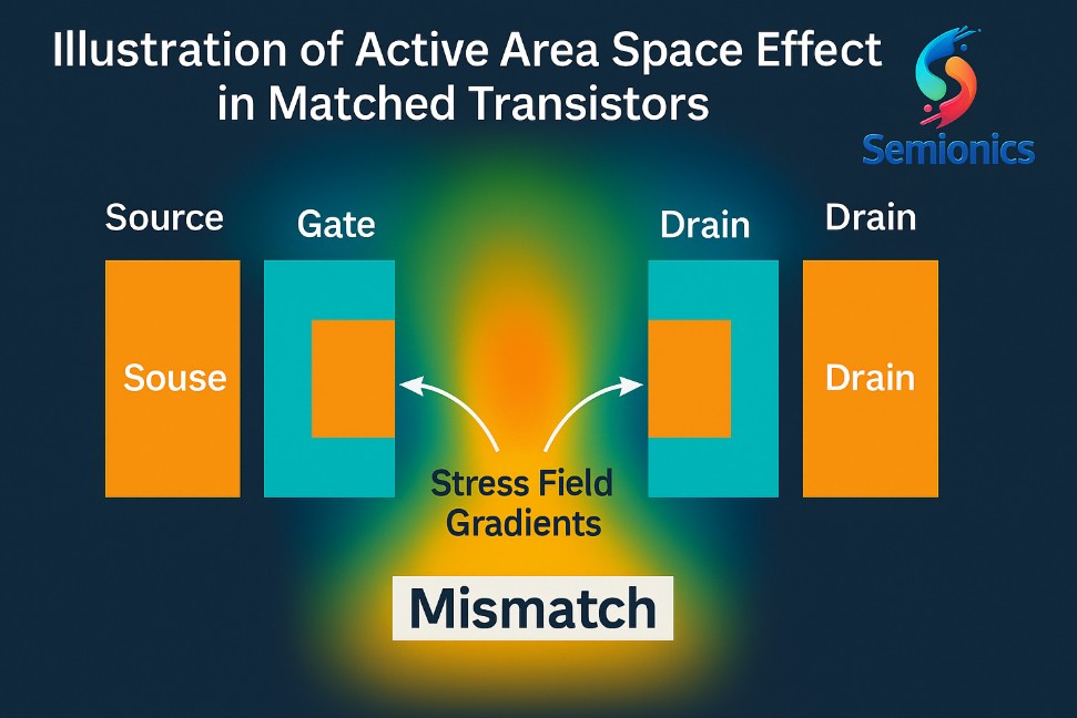
In simple terms, Active Area Space Effect refers to the variation in transistor characteristics caused by non-uniform spacing between diffusion (active) regions. When transistors are placed too close or too far apart, mechanical and thermal stresses induced during fabrication change the local lattice strain, leading to shifts in threshold voltage (Vth), mobility, and current matching. For analog and mixed-signal designers, this means that even identically drawn devices can behave differently once fabricated.
“AAS isn’t visible on your layout screen — but it leaves its fingerprint on every mismatch you measure.”
AAS is particularly destructive in precision circuits such as:
In these cases, the distance between active regions dictates how uniformly devices experience shallow trench isolation (STI) and process-induced stress. When one device sits closer to a field oxide edge, it experiences a different strain environment than its counterpart, leading to mismatches in Vth and Idsat. Even variations of 100–200 nm can introduce offset voltages in the millivolt range — enough to cause gain imbalance or yield loss in analog blocks.
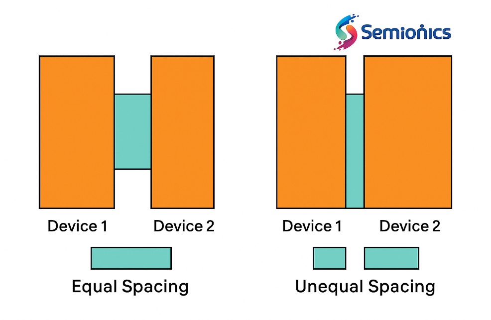
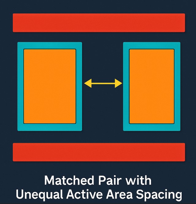
Let’s explore how AAS appears in practical layouts:
Such subtle geometric differences can cumulatively degrade precision, linearity, and temperature stability.
“AAS is a layout-dependent effect that doesn’t break rules — it bends physics.”
Designers can mitigate AAS through smart layout planning and adherence to symmetry principles.
Here are key strategies used by expert layout engineers:
# Maintain Consistent Spacing: Keep uniform distance between all matched diffusion regions.
# Use Dummy Diffusions: Add dummy actives to equalize edge stress and maintain symmetry.
# Balance Isolation Proximity: Place critical devices equidistant from isolation boundaries.
# Employ Common-Centroid Structures: Distribute devices in mirrored and interleaved patterns.
# Use Foundry Layout Dependent Extraction (LDE): Simulate post-layout stress and electrical variations early.
At Semionics Academy, engineers don’t just learn what the Active Area Space Effect is — they learn how to design against it. Through practical layout simulations, live demonstration sessions, and interactive “Layout Nuggets” videos, Semionics bridges the gap between textbook theory and silicon reality. The Academy’s LMS-based learning modules include visual explorations of how AAS influences transistor stress fields, and how dummy actives, spacing control, and layout symmetry can eliminate matching errors before tapeout.
“At Semionics, layout learning is not about drawing rectangles — it’s about mastering the invisible forces that shape silicon.”
With today’s sub-10nm technology nodes, layout-dependent effects (LDEs) like AAS, DLE, and PCE are becoming first-order performance limiters.
Designers who understand these effects design not just faster chips, but reliable ones.
By making engineers aware of the physics behind geometry, Semionics Academy is cultivating a new generation of layout thinkers who can translate micron-level adjustments into millivolt-level precision.
Whether you’re building AI accelerators, mixed-signal interfaces, or low-power analog IP, mastering AAS is one of the most crucial skills to ensure robust silicon yield and parametric consistency.
“The best layouts aren’t just rule-clean — they’re physics-conscious.”
📞 Connect with Semionics
The images and content used in this blog are generated, created, or referenced from Google Images and other educational sources.
They are intended purely for educational and guidance purposes, with no intention of monetization.
All credits belong to the respective owners. Semionics holds no responsibility for third-party content and encourages readers to verify before use.

Semionics, Your Partner in semiconductor space , connecting industry needs with skilled professionals in Analog & Mixed-Signal IC Layout Design and Physical Verification ."from Basics to Brilliance .. A path to Semiconductor Industry!!"