
ntroduction
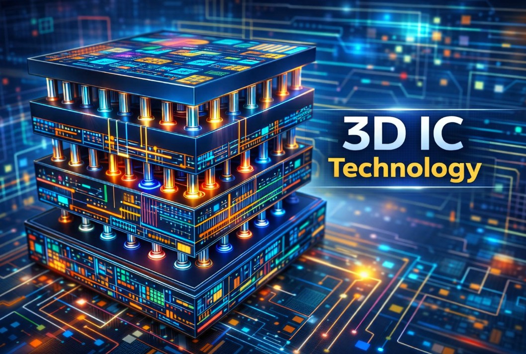
3D Integrated Circuit (3D IC) technology is transforming the way semiconductor chips are designed and manufactured. By vertically stacking multiple layers of circuits, 3D ICs break the limitations of traditional planar designs. This innovation unlocks major improvements in performance, power efficiency, and integration density — making it one of the most significant advances in modern IC development. In this article, we explore the top 5 benefits of 3D IC technology that are driving the future of smart electronics.
One of the primary advantages of 3D IC technology is its ability to significantly improve performance. Traditional 2D designs often suffer from long interconnect delays due to the physical distance between components. In contrast, 3D ICs reduce the distance between interconnected layers, leading to faster signal transmission and higher overall system speed.
Why This Matters:
By stacking circuits vertically and minimizing interconnect lengths, 3D ICs help reduce power consumption. Shorter connections mean less energy is required for signal transmission — translating into better performance per watt.
Key Benefits Include:
3D ICs leverage vertical stacking to house multiple functional blocks within the same footprint that would otherwise require a much larger 2D chip area. This increased integration density enables:
Use Cases:
Wearables, mobile devices, IoT edge modules, and embedded AI accelerators
3D stacking presents new challenges in heat dissipation, but modern 3D IC designs use advanced thermal pathways and heat spreaders to manage temperature effectively. By integrating thermal vias and optimized heat sinks, 3D ICs ensure consistent performance under load.
Thermal Benefits:
3D IC technology offers higher flexibility when integrating heterogeneous components — such as logic, memory, and analog blocks — within a single stack. This enables advanced System-on-Chip (SoC) implementations that deliver:
| Feature | 2D IC | 3D IC |
|---|---|---|
| Integration Density | Limited | High |
| Interconnect Length | Long | Short |
| Power Efficiency | Moderate | Improved |
| Performance | Standard | Enhanced |
| Thermal Challenges | Lower | Manageable with design |
3D IC technology is a major leap forward in semiconductor innovation. From improved performance and power efficiency to unprecedented integration density, 3D ICs are reshaping modern electronics and chip design. As design tools and manufacturing processes continue to evolve, the adoption of 3D ICs will only grow — powering the next generation of smart devices, AI accelerators, and high-performance computing systems.

Semionics, Your Partner in semiconductor space , connecting industry needs with skilled professionals in Analog & Mixed-Signal IC Layout Design and Physical Verification ."from Basics to Brilliance .. A path to Semiconductor Industry!!"