
Analog layout is one of the foundational skills required for designing high-performance integrated circuits (ICs). Unlike digital layout, where logical blocks dominate, analog layout focuses on precision, matching, device symmetry, and parasitic management to achieve reliable performance. This beginner’s guide explains what analog layout is, why it matters, key techniques, and how to get started.
Analog layout refers to the physical placement and routing of components in an analog integrated circuit — a process that translates the schematic design into a manufacturable layout while preserving performance and minimizing signal errors.
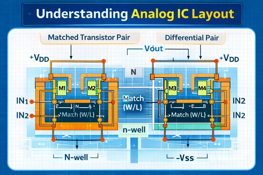
In analog circuits, transistor matching and device symmetry directly affect performance metrics like gain, offset, and linearity.
Good analog layout avoids mismatches that can degrade your design.
Unlike digital designs, where timing dominates, analog circuits are extremely sensitive to parasitic capacitances and resistances — especially at nodes with high impedance. Analog layout tries to control parasitics to maintain signal integrity.
Precise matching of transistors and passive components improves performance.
Common matching techniques include:
These techniques help minimize gradient effects on the silicon.
Guard rings surround sensitive analog blocks to isolate substrate noise and protect high-impedance nodes.
Differential pairs reject common-mode noise and require careful matching and symmetrical routing to work effectively.
Shielding critical nets and isolating analog domains from noisy digital blocks is essential for signal fidelity.
Avoiding these mistakes is key to reliable analog behavior.
Analog layout transforms circuit schematics into real silicon patterns. Its principles are rooted in precision, symmetry, and controllability of parasitics. For beginners, mastering analog layout is a major step toward becoming a competent IC design or layout engineer.
Looking to learn analog layout hands-on?
👉 Explore Semionics’ AMS IC layout courses tailored for beginners and professionals.

Semionics, Your Partner in semiconductor space , connecting industry needs with skilled professionals in Analog & Mixed-Signal IC Layout Design and Physical Verification ."from Basics to Brilliance .. A path to Semiconductor Industry!!"