
Introduction
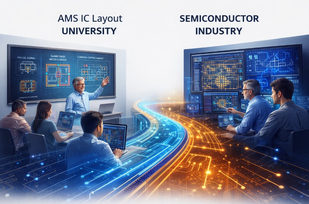
Analog & Mixed Signal (AMS) IC layout is one of the most challenging yet essential skills in semiconductor design. Universities worldwide are recognizing the importance of hands-on training in AMS layout to prepare students for real industry workflows. This article explores how AMS IC layout university training is evolving, why it matters, and how educational institutions can build curricula that bridge the gap between academics and industry demands.
AMS designs combine analog circuitry and digital logic on the same chip, requiring precise layout techniques that ensure matching, noise control, and signal integrity.
Employers increasingly value engineers who not only understand theory but also have practical layout skills with tools and methodologies used in real semiconductor workflows.
Many university programs focus heavily on theory without exposing students to real AMS layout challenges — such as parasitic effects, matching techniques, or DRC/LVS flows.
Access to industry-grade tools (e.g., Cadence Virtuoso, Calibre) is limited in many institutions due to cost and licensing challenges.
True mastery requires practical exposure to physical layout tasks, from device matching to shielding and routing high-impedance nets.
Curriculum should include essential topics such as:
Faculty training and exposure to industry practices helps them deliver relevant and up-to-date coursework.
Organizations like Semionics help universities upgrade curriculums by providing faculty training and industry-grade labs.
Assignments with real AMS IC layout problems (e.g., differential pairs, common-centroid layouts) help students develop practical skills.
Incorporate lab reviews, student feedback loops, and regular updates to course content to keep pace with industry changes.
📞 Connect with Semionics
🎥 YouTube Channel: Subscribe
🌐 Website: www.semionics.com
📚 LMS / Online Learning Platform: academy.semionics.com
🔗 LinkedIn Page: Follow Us
💬 WhatsApp Group: Join Now

Semionics, Your Partner in semiconductor space , connecting industry needs with skilled professionals in Analog & Mixed-Signal IC Layout Design and Physical Verification ."from Basics to Brilliance .. A path to Semiconductor Industry!!"