FinFET – Overcoming Double Patterning Challenges
Introduction In today’s advanced semiconductor industry, FinFET technology has emerged as the backbone of modern integrated circuits. As devices continue
 semionics
- September 29, 2025


Introduction In today’s advanced semiconductor industry, FinFET technology has emerged as the backbone of modern integrated circuits. As devices continue
 semionics
Introduction Power consumption has become one of the most pressing challenges in semiconductor design. With the rise of wearable devices,
semionics
The semiconductor industry is rapidly evolving, and IC Layout Design stands at the heart of this transformation. For engineers stepping
semionics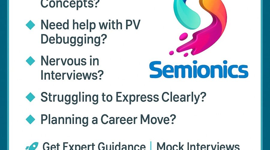
In the fast-paced world of semiconductors and microelectronics, every engineer encounters challenges. Many VLSI professionals find themselves struggling with IC
semionics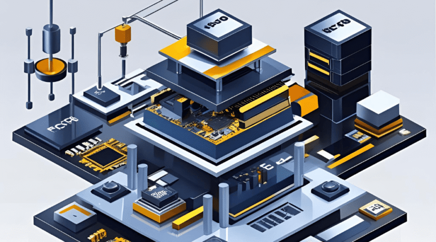
Introduction In the ever-evolving semiconductor landscape, IP Design Services companies are foundational players. They create reusable, high-performance blocks of logic
semionics
Introduction In the world of microelectronics and semiconductor innovation, Electronic Design Automation (EDA) companies play a silent yet transformative role.
semionics
In the world of VLSI design and semiconductor engineering, ensuring that a chip is both manufacturable and functionally correct is
semionics
In today’s semiconductor industry, where precision and performance drive innovation, Cadence Virtuoso stands as the gold standard for analog and
semionics