
In the world of semiconductor design, mastering analog layout matching techniques is essential for building high-performance analog and mixed-signal integrated circuits (ICs). These techniques ensure that paired devices behave consistently — a crucial factor for precision, low noise, and performance. This comprehensive guide demystifies the core concepts and practical methods every IC layout engineer should know.
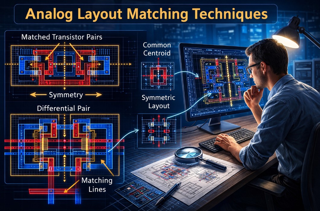
Analog layout matching refers to the practice of placing and routing transistors and passive components in a way that ensures their electrical characteristics stay as similar as possible. This is critical for circuits like differential amplifiers, current mirrors, and precision references.
If transistors in a differential pair are not matched properly, mismatches can lead to offsets, gain errors, and even oscillations.
Poor matching can introduce unintended parasitic effects, degrading signal integrity and overall performance.
A standard technique where matched devices are interleaved to minimize gradient effects across the silicon.
Placed in alternating order, devices are connected in a way that balances systematic variability.
Ensures that devices see similar environmental and process conditions — critical for high-precision circuits.
Using multi-finger structures can improve matching and reduce parasitic resistance and capacitance.
Consistent routing — especially in differential and current-mode circuits — maintains symmetry and minimises mismatch.
Understanding proximity effects, such as stress and density variations, helps refine matched layouts.
Build real-world analog layout skills with hands-on training and expert mentorship.
👉 Explore Semionics’ Analog IC Layout Programs and take your career to the next level.
This session is tailored for undergraduate students, master’s & Ph.D. researchers, and experienced layout professionals. Whether you’re just starting out or need to refine your matching strategies, this hands-on course will take your skills to the next level.
You’ll learn:
Semionics courses are designed by working semiconductor professionals, offering unmatched insights into real-world design flows.
⭐⭐⭐⭐⭐ “The Matching Techniques session changed how I approach layout. I landed an internship thanks to this training.”
⭐⭐⭐⭐⭐ “I shared this course with my entire project team. The common centroid demo was a game-changer.”
⭐⭐⭐⭐⭐ “From dummy insertion to dispersion control — everything was practically explained. Semionics LMS is brilliant!”
We encourage learners to explore our full range of IC Layout courses, including:

📚 Share these sessions with your peers and colleagues — help grow the VLSI community with Semionics Academy.

Semionics, Your Partner in semiconductor space , connecting industry needs with skilled professionals in Analog & Mixed-Signal IC Layout Design and Physical Verification ."from Basics to Brilliance .. A path to Semiconductor Industry!!"