

The semiconductor industry is at the heart of modern technology. For decades, the design philosophy centered on building larger and more complex monolithic SoCs (System-on-Chips). However, as Moore’s Law slows and manufacturing costs escalate, a new paradigm has emerged: chiplets.
Today, chiplet-based architectures are not just a trend; they are becoming the foundation of AI accelerators, high-performance computing (HPC), cloud servers, and automotive electronics. Let’s take a closer look at why chiplets matter, how they are designed, and what challenges and opportunities they bring for semiconductor professionals.
Instead of creating one massive SoC, engineers now disaggregate functionality into smaller, reusable blocks called chiplets. Each chiplet performs a specific role—such as CPU cores, memory controllers, or I/O interfaces—and can be combined with others using advanced packaging technologies like 2.5D ICs, 3D ICs, and silicon interposers.
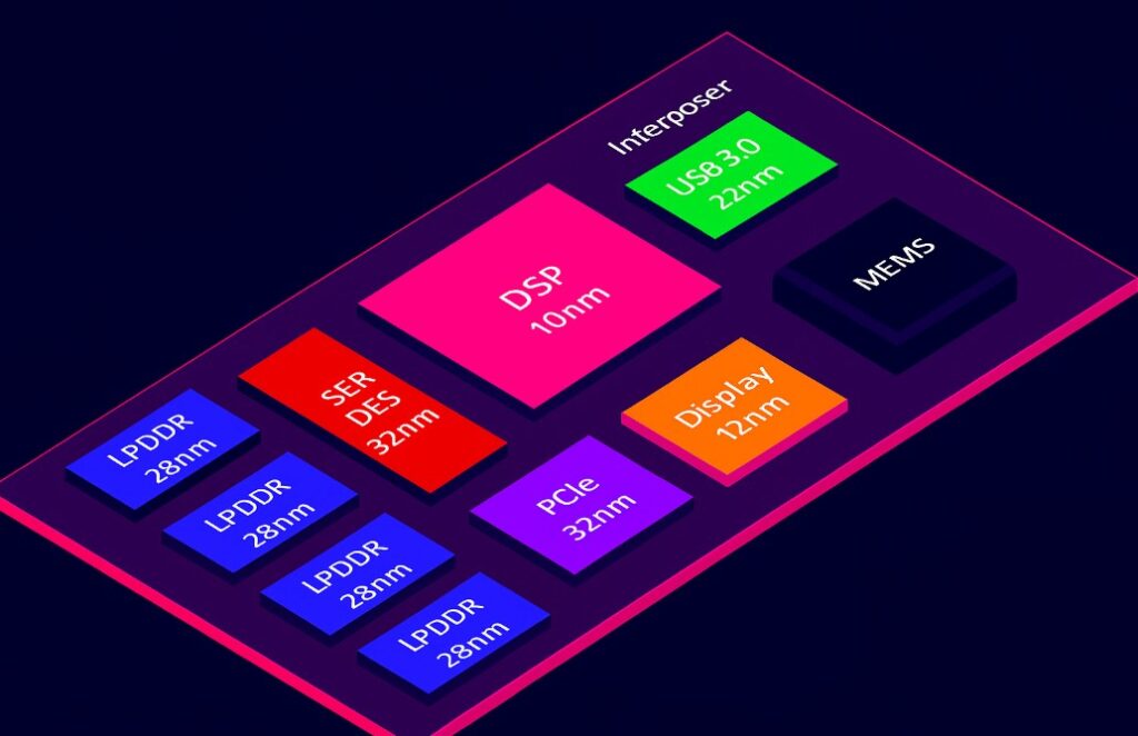
✔ Flexibility: Chiplet-based systems allow companies to mix-and-match IPs across different technology nodes. For instance, compute-intensive logic may sit on 5nm or 7nm, while analog or I/O functions stay on mature 28nm or 65nm nodes.
✔ Cost-Efficiency: Instead of re-designing everything from scratch, companies reuse proven silicon blocks. This reduces development time and improves yield.
✔ Scalability: By adding or swapping high-speed chiplets, manufacturers can scale performance rapidly—vital in AI, cloud computing, and 5G applications.
While the benefits are clear, chiplet integration comes with its own set of challenges.
🔹 Die-to-Die Interfaces: Seamless communication across chiplets is not trivial. Engineers must ensure high bandwidth, low latency, and protocol compatibility.
🔹 Power Integrity & Thermal Management: With multiple chiplets operating together, power delivery networks and heat dissipation become more complex than traditional SoCs.
🔹 Yield & Packaging Complexity: Advanced assembly in 2.5D and 3D IC packaging requires extremely high precision. Even a small defect in one chiplet can affect the entire system.
🔹 Standardization & Interoperability: Industry standards like UCIe (Universal Chiplet Interconnect Express) aim to simplify cross-vendor chiplet integration. However, true interoperability across the semiconductor supply chain remains a work in progress.

Chiplets are versatile across multiple semiconductor nodes. For example:
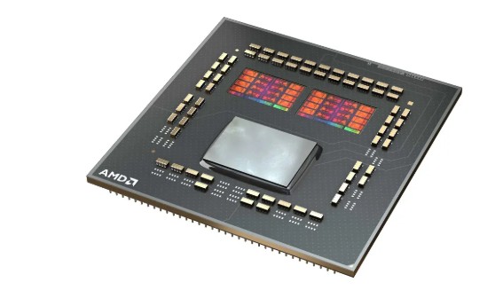
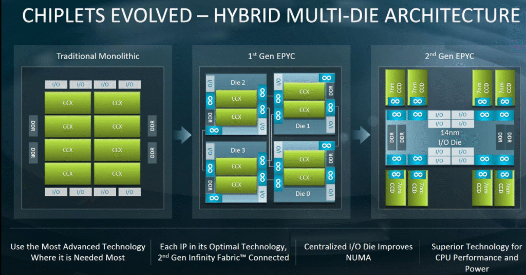
Some notable chiplet-based products include:
(Insert Picture: Comparative infographic of AMD EPYC, Intel Sapphire Rapids, and Apple M1 Ultra chiplet diagrams)
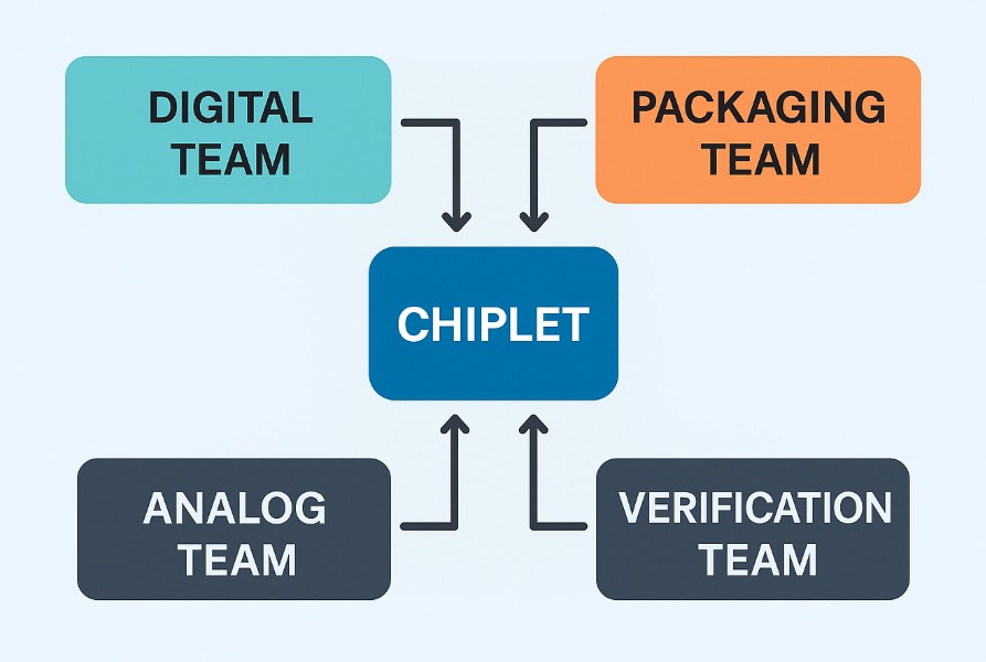
For engineers, the chiplet revolution is rewriting the design workflow.
This shift is also reshaping the skills required in the industry. Aspiring engineers must gain exposure not just to ASIC back-end design, but also to system-level co-design methodologies.
The chiplet ecosystem is still evolving, but one thing is certain: it represents the future of semiconductor architecture. With leaders like AMD, Intel, TSMC, and Apple driving innovation, the industry is steadily moving toward modular, scalable, and cost-efficient designs.
For professionals, chiplets open opportunities in packaging technologies, heterogeneous integration, and system co-optimization. For students and aspiring engineers, they offer an exciting entry point into the next generation of microelectronics.
If you want to stay ahead of the curve, now is the time to build your chiplet expertise.
At Semionics, we are committed to making VLSI education accessible worldwide. Whether you are a student, working professional, or faculty member, our resources will help you explore the world of chiplets, advanced packaging, and semiconductor design.
👉 Stay connected with us through the following:

Semionics, Your Partner in semiconductor space , connecting industry needs with skilled professionals in Analog & Mixed-Signal IC Layout Design and Physical Verification ."from Basics to Brilliance .. A path to Semiconductor Industry!!"