Lithography 2025: The Next Frontier in Semiconductor Manufacturing

Shape Image One
Lithography 2025: The Next Frontier in Semiconductor Manufacturing

As we approach 2025, the world of semiconductor lithography stands at a pivotal crossroads. The technology that etches microscopic circuits onto silicon wafers is undergoing its most significant transformation in decades, promising to unlock new possibilities in computing power, energy efficiency, and technological innovation.

The Current Landscape: Where We Are Today

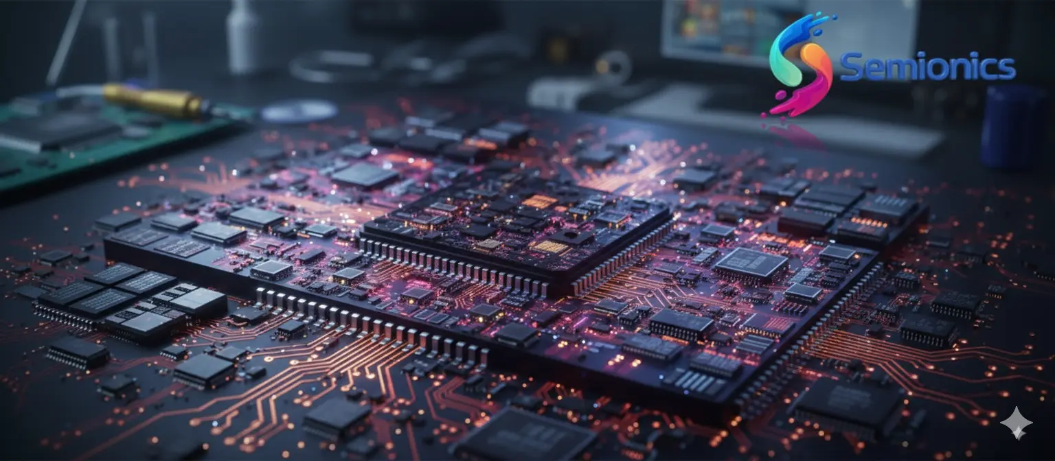
Modern lithography has become the cornerstone of semiconductor manufacturing, determining how small and efficient we can make transistors. Current state-of-the-art systems use Extreme Ultraviolet (EUV) lithography with 13.5nm wavelength light to create features as small as 3-5 nanometers. That’s like drawing lines 20,000 times thinner than a human hair!

Leading chip manufacturers like TSMC, Samsung, and Intel are already using these advanced systems to produce the processors powering everything from smartphones to supercomputers. But as we look toward 2025, even more revolutionary changes are on the horizon.

High-NA EUV: The Game Changer for 2025

The most anticipated development in 2025 lithography is the widespread adoption of High-Numerical Aperture (High-NA) EUV technology. This isn’t just an incremental improvement—it’s a fundamental leap forward.

What Makes High-NA Special:

  • Higher resolution capabilities for features below 2nm
  • Reduced pattern complexity through single-exposure patterning
  • Improved yield and manufacturing efficiency
  • Lower overall cost per chip at advanced nodes

ASML, the Dutch company that dominates the EUV landscape, has already begun shipping its first High-NA EUV systems to major chip manufacturers. These machines stand three stories tall, cost over $300 million each, and represent the pinnacle of precision engineering.

The 2025 Technology Stack: What’s Coming Online

Multi-Beam Mask Writing

Creating the photomasks for advanced lithography is becoming increasingly challenging. In 2025, we’ll see wider adoption of multi-beam mask writing technology that can:

  • Reduce mask writing time from days to hours
  • Improve pattern accuracy and resolution
  • Enable more complex designs with fewer defects

Advanced Pattern-Shaping Techniques

Computational lithography is evolving rapidly, with 2025 bringing:

  • AI-powered inverse lithography technology (ILT)
  • Real-time pattern correction and optimization
  • Machine learning-driven hotspot detection
  • More sophisticated source-mask optimization

Materials Innovation

The lithography materials ecosystem is keeping pace with new developments:

  • Next-generation photoresists with higher sensitivity
  • Improved underlayers for better pattern transfer
  • Advanced hard masks and multiple patterning schemes

Industry Impact: Who Benefits and How

Chip Manufacturers

For companies like TSMC and Intel, 2025 lithography advances mean:

  • Ability to maintain Moore’s Law progression
  • Competitive advantage in the 2nm and below race
  • More cost-effective manufacturing at leading nodes
  • Faster time-to-market for advanced designs

Equipment Suppliers

The lithography equipment market is poised for significant growth:

  • ASML continues to dominate High-NA EUV
  • Japanese companies like Nikon and Canon focusing on specialty applications
  • Smaller players innovating in adjacent technologies
  • Increased demand for metrology and inspection tools

Chip Designers

For companies designing the next generation of processors:

  • Greater design flexibility with smaller features
  • Reduced reliance on complex multi-patterning
  • New opportunities for architectural innovation
  • Better performance and power characteristics

Challenges on the Horizon

Despite the exciting advancements, 2025 lithography faces significant hurdles:

Technical Barriers

  • Managing stochastic effects and randomness at atomic scales
  • Controlling line-edge roughness and local CD variation
  • Overcoming quantum effects in ultra-small features
  • Ensuring pattern fidelity across entire wafers

Economic Considerations

  • Soaring equipment costs requiring unprecedented capital investment
  • Rising R&D expenses for process development
  • Need for massive scaling to justify investments
  • Increasing complexity of supply chain management

Workforce Development

  • Shortage of experienced lithography engineers
  • Need for cross-disciplinary expertise
  • Rapidly evolving skill requirements
  • Global competition for top talent

The Global Landscape: Geopolitical Implications

Lithography technology has become a strategic asset in global technology competition:

Export Controls and Restrictions:

  • Ongoing limitations on advanced lithography equipment exports
  • Impact on global semiconductor supply chains
  • National security considerations driving policy decisions

Regional Development Initiatives:

  • China’s push for domestic lithography capabilities
  • European efforts to maintain technology leadership
  • US investments in domestic semiconductor manufacturing

Sustainability and Environmental Considerations

As lithography advances, environmental impact becomes increasingly important:

Energy Consumption:

  • EUV systems require massive power inputs
  • Cooling and facility requirements adding to energy loads
  • Industry focus on improving energy efficiency

Materials and Waste:

  • Managing chemical waste from photoresist processing
  • Recycling and reuse initiatives gaining importance
  • Development of more environmentally friendly processes

Looking Beyond 2025: What’s Next?

While 2025 represents a major milestone, the industry is already looking further ahead:

Hyper-NA EUV Development:

  • Research into next-generation NA values
  • Potential for single-digit atomic scale patterning
  • New physics and engineering challenges

Alternative Technologies:

  • Nanoimprint lithography for specific applications
  • Directed self-assembly research continuing
  • Electron beam and other non-optical approaches

Quantum and Neuromorphic Applications:

  • Specialized lithography requirements for quantum chips
  • Unique patterning needs for neuromorphic computing
  • Customized approaches for emerging computing paradigms

Getting Ready for the 2025 Lithography Revolution

For professionals and students interested in this field:

Educational Pathways:

  • Advanced degrees in electrical engineering and materials science
  • Specialized courses in semiconductor manufacturing
  • Hands-on experience through internships and co-op programs

Career Opportunities:

  • Process integration engineers
  • Lithography equipment specialists
  • Computational lithography experts
  • Materials and chemistry researchers

Staying Informed:

  • Following industry conferences like SPIE Advanced Lithography
  • Monitoring technical publications and patent filings
  • Engaging with professional organizations and networks

Conclusion: Why 2025 Matters

The lithography advancements coming in 2025 represent more than just technical progress—they enable the next generation of technological innovation. From artificial intelligence and autonomous vehicles to medical breakthroughs and sustainable energy solutions, all these technologies depend on the continued advancement of semiconductor manufacturing.

As we approach this pivotal year, the entire semiconductor ecosystem—from equipment manufacturers to chip designers to end users—must prepare for the opportunities and challenges that advanced lithography will bring. The companies and countries that successfully navigate this transition will likely lead the next wave of technological innovation.

How Semionics Can Help You

At Semionics, we provide hands-on training, industry exposure, and mentorship for engineers aspiring to enter analog VLSI jobs. Our programs cover design, layout, EDA methodologies, and verification.

📞 Contact: +91-8904212868

🌐 Website: www.semionics.com

📚 LMS / Online Learning Platform: academy.semionics.com

🔗 LinkedIn Page: Follow Us

💬 WhatsApp Group: Join Now

🎥 YouTube Channel: Subscribe

📧 Email: enquiry@semionics.com

Leave a Reply

Your email address will not be published. Required fields are marked *