

The semiconductor industry in India is experiencing unprecedented growth, fueled by government initiatives, global investments, and a rising demand for skilled professionals. However, a critical challenge persists—the gap between academic VLSI education in India and industry requirements. While colleges provide strong theoretical foundations, they often fall short in delivering hands-on exposure to EDA tools, semiconductor design workflows, and real-world project practices.
This gap not only slows down employability but also prevents young engineers from becoming industry-ready immediately after graduation. Let us explore why this disconnect exists and how innovative platforms like Semionics are redefining VLSI training in India.
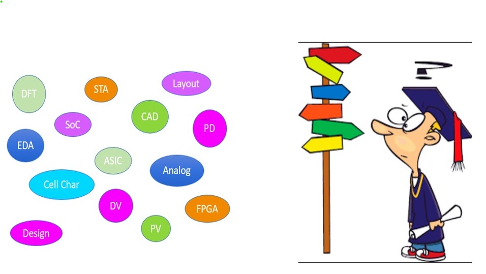
Engineering colleges across India produce thousands of graduates each year with degrees in electronics, semiconductor, and microelectronics. Unfortunately, many graduates are unaware of the latest ASIC design flows, AMS layout methodologies, or FinFET-specific challenges. Courses often remain focused on theory, with limited access to EDA tools such as Cadence, Synopsys, or Mentor Graphics.
Without practical semiconductor courses online, students miss the opportunity to practice Digital and Analog layout skills ,CMOS, Finfet, and advanced low-power design techniques—all of which are essential in today’s chip design ecosystem.
The result? A significant skill mismatch. Companies spend months re-training new hires to make them project-ready.
The semiconductor industry is highly dynamic. With Moore’s Law slowing down, the move toward FinFETs, GAAFETs, and 3D IC packaging is reshaping chip design. To stay relevant, engineers need practical skills in cutting-edge EDA tools and layout flows.
This is where industry-ready VLSI courses make a difference. They integrate hands-on training, project-based learning, and exposure to advanced design methodologies. Such training empowers engineers to confidently handle analog layout, timing closure, verification, and sign-off checks—key stages that directly impact tape-out success.
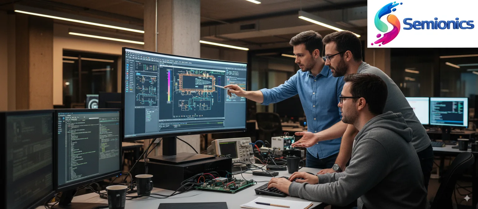
Semionics, through its LMS-driven semiconductor courses online, is focused on bridging the gap between colleges and industry. By combining real-world design expertise with structured learning paths, it offers one of the best VLSI training platforms in India and abroad.
Key highlights include:
This approach ensures that students are not just learning concepts but are also becoming job-ready semiconductor professionals.
Visit the career counselling free sessions on Semionics academy :
click the link : https://academy.semionics.com/s/store/courses/CAREER%20COUNSELLING
The future of VLSI education in India lies in building a collaborative ecosystem. Universities must strengthen their industry partnerships, while online platforms like Semionics will continue to accelerate access to high-quality, industry-relevant courses.
With India aiming to be a global semiconductor hub, the demand for trained talent in chip design, verification, and analog layout will only rise. Aspiring engineers who invest in specialized VLSI training platforms today will be at the forefront of tomorrow’s semiconductor revolution.
Bridging the gap between academic training and industry expectations is no longer optional—it is the only way forward. The semiconductor industry demands engineers who can design, verify, and implement complex chips with precision. With platforms like Semionics leading the charge, India is set to redefine its place in the global semiconductor value chain.
The images and content used in this blog are generated, created, or referenced from Google Images and other educational sources. They are intended purely for educational and guidance purposes, with no intention of monetization. All credits belong to the respective owners. Semionics holds no responsibility for third-party content and encourages readers to verify before use.

Semionics, Your Partner in semiconductor space , connecting industry needs with skilled professionals in Analog & Mixed-Signal IC Layout Design and Physical Verification ."from Basics to Brilliance .. A path to Semiconductor Industry!!"